PCB Fabrication Laboratory
The PCB lab is a state of the art laboratory used to fabricate PCBs and antenna. Printed circuit boards are electronic circuits boards created for mounting electronic components on a nonconductive board, and creating conductive connections between them. The creation of circuit patterns is accomplished by using both additive and subtractive methods. The conductive circuit is generally copper, although aluminum, nickel, chrome, and other metals are sometimes used.
Laboratory Facilities
| Sl. No. | Name of the facility | Specifications |
|---|---|---|
| 1 | PCB Artwork Film Maker (NV180) | 230 V / 50 Hz, 16 × 2 LCD for timer and lamp status display |
| 2 | Artwork Table (NV181) | 230 V / 50 Hz |
| 3 | PCB Shearing Machine (NV182) | Table Mounted / Floor Mounted |
| 4 | Photoresist Dip Coating Machine (NV183) | 230 V / 50 Hz, 16 × 2 LCD for timer |
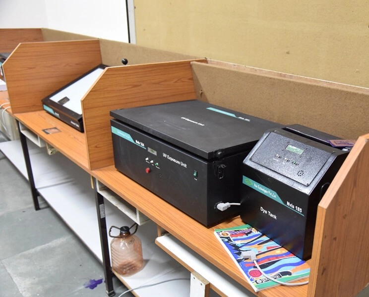
| 5 | UV Exposure Unit (NV184) | 230 V / 50 Hz, 16 × 2 LCD for timer and lamp status display |
| 6 | Dye Tank (NV185) | 230 V / 50 Hz, 16 × 2 LCD for timer |
| 7 | Development Tank (NV186) | 230 V / 50 Hz, 16 × 2 LCD for timer |
| 8 | PCB Etching Machine (NV187) | 230 V / 50 Hz, Spray Etching machine, Automatic / Manual |
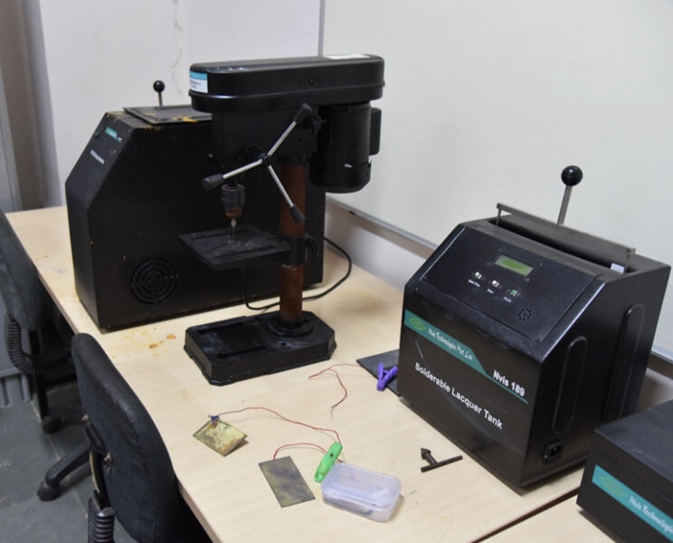
| 9 | Drill Machine (NV188) | 230 V / 50 Hz, 1500 which are adjustable in steps |
| 10 | Solderable Lacquer Tank (NV189) | 230 V / 50 Hz, 16 × 2 LCD for timer |
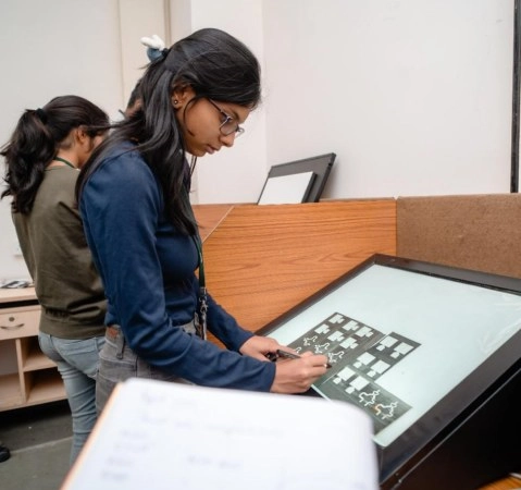
| 11 | PCB Designer Kit (NV190) | Marker pens, stencils, scales, drafting aids |
| 12 | PCB Curing Machine (NV191) | 230 V / 50 Hz |
| 13 | Chemicals |